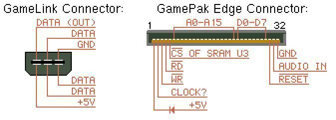
for #4, the pins are all just labeled with the name of the node, usually taken from a schematic. When talking about (and making) schematics, 'node' means any continuous line on the schematic (or metal conductor in reality). So nodes can each be named anything, If you are solving stuff with circuit equations you might just call them x and y, or v1 and v2. Usually any nodes hooked up to an integrated circuit will take on the name of the pin that they are connected to. All integrated circuits have names for all of their pins, given in the datasheet.
The point is, the labels on the pins in that diagram are specific to the integrated circuits that they are attached to. In the second image, I see a chip select (CS), read (RD) and write (WR) lines, which makes sense because it says its connected to some SRAM, and all SRAM chips have those pins. All the answers are in the datasheet specific to your integrated circuits.
I hope thats not confusing
Also, logic timing diagrams like this, taken from an n64 cart bus, help people understand how the signals relate to each other. This is similar to the output you would get from a logic analyzer.
http://crazynation.org/N64/n64_cart_info.htm" onclick="window.open(this.href);return false;