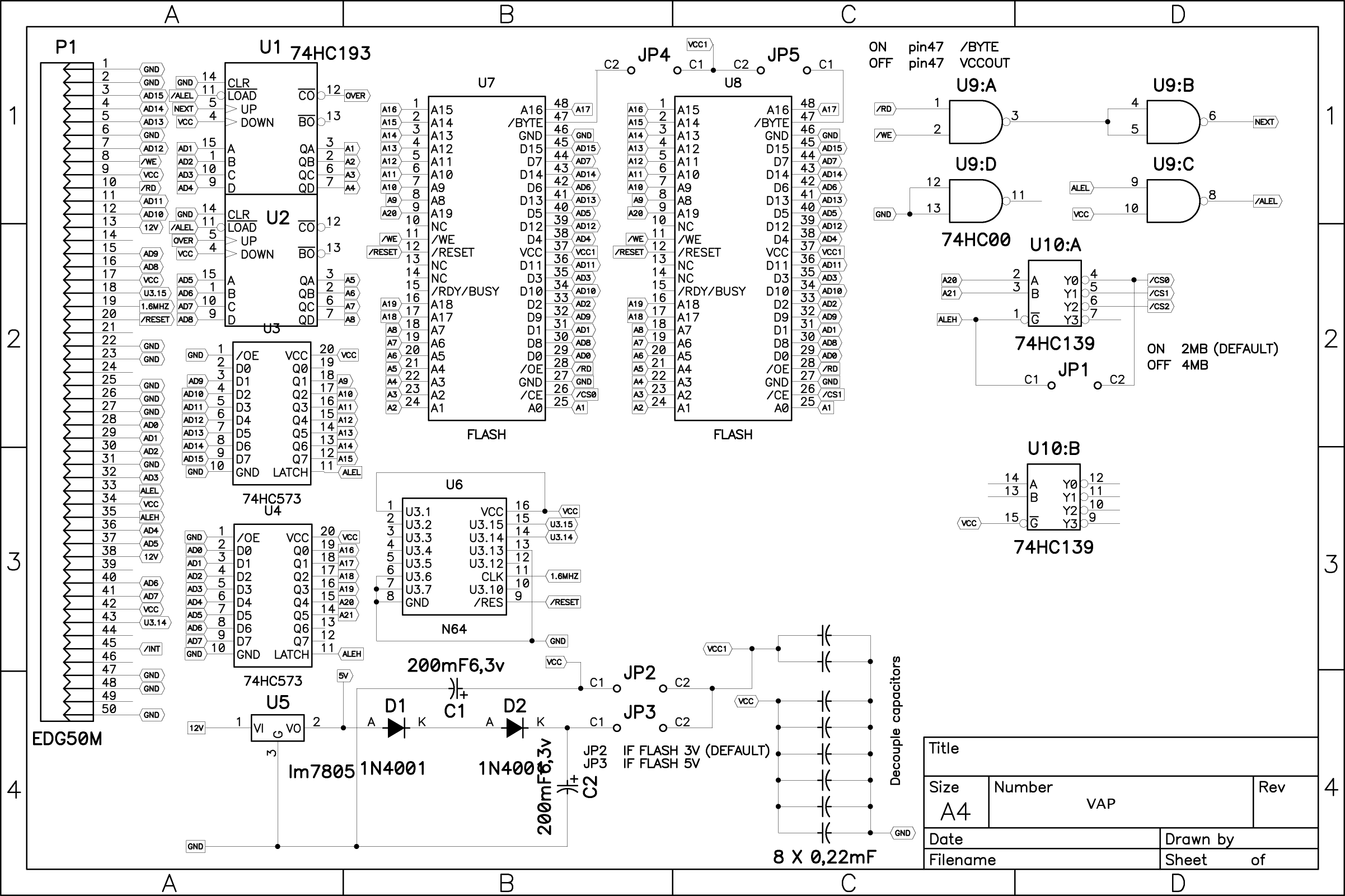
Yes, it will be similar, but the AT49 flash chip you mentioned only operates in 16-bit mode. This means you need fewer address lines, but you need 16 data lines instead of just 8 (the SRAM example has 8 )
The ATmega32 would work, except it doesn't have enough I/O pins to drive all the address and data pins of the Flash ROM.
For FlashROM you need to write some commands before you write a block.
For example, my code was
Code: Select all
// write to ROM
		writeROMByte(0xAA, 0x5555);
		writeROMByte(0x55, 0x2AAA);
		writeROMByte(0xA0, 0x5555);
		writeROMByte('p', 0);
		writeROMByte('a', 1);
		writeROMByte('g', 2);
		writeROMByte('e', 3);
		writeROMByte('d', 4);
		writeROMByte('1', 5);
		writeROMByte('u', 6);
		writeROMByte('p', 7);
Now back to your problem.
If you look at the AT49BV642d datasheet, it has 22 address lines, and 16 I/O lines. You only have 24 I/O lines available on the ATmega.
For the address lines, you will only be outputting to them with the microcontroller. So, you can use a shift register.
http://www.allaboutcircuits.com/vol_4/chpt_12/4.html" onclick="window.open(this.href);return false;
Try this one:
http://www.fairchildsemi.com/ds/74/74VHC164.pdf" onclick="window.open(this.href);return false;
You have 22 address lines, so you need 3 of these chips. Tie the B input high and only use the A input. Connect all three A inputs together. This goes to an I/O on your ATmega. Now use three more I/O for the CP inputs.
So now you have 22 address lines reduced to 4 I/O. That will work fine

Now you have to modify the source code to work with this arrangement. But it is possible.